Transistor: Difference between revisions
From DT Online
Added transistor types |
mNo edit summary |
||
| (9 intermediate revisions by the same user not shown) | |||
| Line 1: | Line 1: | ||
[[File:Transistor2.jpg| | [[File:Transistor2.jpg|350px|right]] | ||
__TOC__ | |||
=====Description===== | |||
[http://en.wikipedia.org/wiki/Transistor '''Transistors'''] are used as electronic ''[[switches]]'' and current amplifiers. They have three ‘legs’ - base , collector and emitter. A small current to the base switches on the transistor allowing a much larger current to flow between collector and emitter. | [http://en.wikipedia.org/wiki/Transistor '''Transistors'''] are used as electronic ''[[switches]]'' and current amplifiers. They have three ‘legs’ - base , collector and emitter. A small current to the base switches on the transistor allowing a much larger current to flow between collector and emitter. | ||
| Line 14: | Line 19: | ||
[https://en.wikipedia.org/wiki/Bipolar_junction_transistor#NPN '''NPN transistors'''] are most commonly used in schools for control circuits. | [https://en.wikipedia.org/wiki/Bipolar_junction_transistor#NPN '''NPN transistors'''] are most commonly used in schools for control circuits. The Base and Collector need to be positive with respect to the Emitter and a base voltage of at least 0.6V with respect to the emitter to ‘turn on’ ''([http://en.wikipedia.org/wiki/Darlington_transistor '''Darlington Pair transistors'''] require 1.2 V)''. A limiting resistor - typically 1K is required in the base circuit of the transistor stage to prevent over-running and hence overheating and destruction of the transistor. | ||
| Line 20: | Line 25: | ||
<div style="clear: both;"></div> | <div style="clear: both;"></div> | ||
[https://en.wikipedia.org/wiki/Bipolar_junction_transistor#PNP '''PNP transistors'''] need the Collector and Base to be negative with respect to the Emitter and ‘turn on’ when the base current falls below 0.6V with respect to the emitter. | |||
[ | =====Transistor Formulae===== | ||
[[File:TransistorGainCalc.png|300px|right]] | |||
The current gain of a transistor (hFE) is the ratio of the current flowing through the collector, to the current flowing through the base. It is a measure of the transistor's ability to amplify current. | |||
| Line 28: | Line 37: | ||
Transistors were developed as the result of some work at the [http://en.wikipedia.org/wiki/Bell_Labs '''Bell Telephone Labs.'''] in 1948 by a team comprising [http://en.wikipedia.org/wiki/William_Shockley '''William Shockley, John Bardeen and Walter Houser'''] - in 1956 the team were jointly awarded a [http://en.wikipedia.org/wiki/Nobel_Prize_in_Physics '''Nobel Prize in Physics'''] for this work. | Transistors were developed as the result of some work at the [http://en.wikipedia.org/wiki/Bell_Labs '''Bell Telephone Labs.'''] in 1948 by a team comprising [http://en.wikipedia.org/wiki/William_Shockley '''William Shockley, John Bardeen and Walter Houser'''] - in 1956 the team were jointly awarded a [http://en.wikipedia.org/wiki/Nobel_Prize_in_Physics '''Nobel Prize in Physics'''] for this work. | ||
The main material, silicon, can be made into a conductor by '''''doping''''': a process of adding impurities to the silicon crystal. Adding phosphorus or arsenic creates N-type Silicon ''(negatively charged)'' whereas adding boron or gallium produces P-type Silicon ''(positively charged)''. | The main material, silicon, can be made into a conductor by '''''doping''''': a process of adding impurities to the silicon crystal. Adding phosphorus or arsenic creates N-type Silicon ''(negatively charged)'' whereas adding boron or gallium produces P-type Silicon ''(positively charged)''. | ||
Combining layers of the two types of silicon side by side produces a '''[[Diode]]'''. The transistor is essentially a [https://en.wikipedia.org/wiki/Triode '''Triode'''] built up from a thin central layer of one type of silicon semiconductor sandwiched between two thicker pieces of the other type - i.e. either NPN or PNP. | Combining layers of the two types of silicon side by side produces a '''[[Diode]]'''. The transistor is essentially a [https://en.wikipedia.org/wiki/Triode '''Triode'''] built up from a thin central layer of one type of silicon semiconductor sandwiched between two thicker pieces of the other type - i.e. either NPN or PNP. | ||
=====Transistor Equivalents===== | |||
It is not always possible to find exactly the same [https://en.wikipedia.org/wiki/Transistor '''Transistor'''] as specified in projects but, since most '''Transistors''' used in '''[[Design and Technology]]''' are '''General Purpose Transistors''', substitutes can usually be found quite easily | |||
Tables of substitutes are available from manufacturers or can be searched for using the internet. The main variables to check are : | |||
* the voltages and current that the '''Transistor''' needs to accommodate; | |||
** '''IC max.''' is the maximum Collector current ''(choose a value which is at least as high as the '''Transistor''' being substituted)''. | |||
** '''VCE max.''' is the maximum current across the Collector-Emitter junction ''(for the low power circuits used in '''D&T''' this can usually be ignored)'' | |||
** '''hFE''' is the Current Gain ''(this value is really only of interest to advanced users)'' | |||
** '''Ptot max.''' is the maximum total power that can be handled by the '''Transistor''' ''(it is of interest in amplification circuits but in switching circuits, '''IC max.''' is a better guide)'' | |||
* the pin-out or relative positions of the '''Base''', '''Collector''' and '''Emitter''' ''(although even if different, there is often a long enough wire 'tail' to allow them to be bent into place)''; | |||
* the design of the case ''(but only if the physical space occupied by the '''Transistor''' is an issue). | |||
Most '''Transistors''' used in '''[[Design and Technology]]''' begin with '''B''' ''(Silicon)'' as in BC108 or BFY51 or '''TIP''' ''(Texas Instruments Power)'' as in TIP120 - other manufacturers use their own codes ''(e.g. ZTX is used by Ferranti)''. '''2N''' as in 2N3053 simply identifies the component as a '''Transistor''' ''(as opposed to '''1N''' for '''[[Diode]]''' as in 1N4001)'' - see [http://en.wikipedia.org/wiki/Pro_Electron '''Pro Electron'''] and [http://en.wikipedia.org/wiki/JEDEC '''JEDEC'''] numbering systems. Any second letter specifies a particular type and this is follows by the serial number of the device ''(three numbers for domestic use)''. If a letter is added at the end, this simply identifies a special version of the main type ''(e.g. a different case style)''. In addition there is also [https://en.wikipedia.org/wiki/JIS_semiconductor_designation '''Japanese Industrial Standards ''(JIS)'''''] coding which may be found on some components. | |||
The packaging or case type used to house a [https://en.wikipedia.org/wiki/Transistor '''Transistor'''] varies and is mainly dependent on how much power needs to be dissipated ''(e.g larger cases can dissipate more heat and metal cases can be coated with with heat conducting grease and mounted on to a '''Heat Sink''' to keep them cool)''. Common [https://en.wikipedia.org/wiki/List_of_integrated_circuit_packaging_types '''Packaging Types'''] encountered in '''[[Design and Technology]]''' are: [https://en.wikipedia.org/wiki/TO-5 '''TO-5''' ''(ie. Transistor Outline 5)'']; [https://en.wikipedia.org/wiki/TO-18 '''TO-18''']; [https://en.wikipedia.org/wiki/TO-92 '''TO-92''']; [https://en.wikipedia.org/wiki/TO-220 '''TO-220'''] and [https://en.wikipedia.org/wiki/TO-3 '''TO-3''']. | |||
{{Transistor & IC Buyers Guide}} | |||
[[Category:Secondary]] | [[Category:Secondary]] | ||
[[Category:Electronics | [[Category:Electronics Components]] | ||
Latest revision as of 07:34, 4 July 2016

Description
Transistors are used as electronic switches and current amplifiers. They have three ‘legs’ - base , collector and emitter. A small current to the base switches on the transistor allowing a much larger current to flow between collector and emitter.
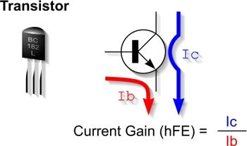
The current gain of a transistor (hFE) is the ratio of the current flowing through the collector, to the current flowing through the base. It is a measure of the transistor's ability to amplify current (hFE = Ic/Ib).
They come in various different shapes and sizes and it is important to decide which type is required at the outset. Factors to be considered are voltage and power handling capacities, cost and availability.
Transistor Types
Transistors come in NPN and PNP types. It is important to use the correct type when designing and building circuits.
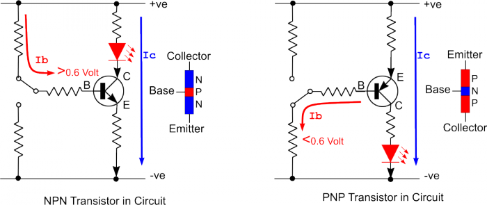
NPN transistors are most commonly used in schools for control circuits. The Base and Collector need to be positive with respect to the Emitter and a base voltage of at least 0.6V with respect to the emitter to ‘turn on’ (Darlington Pair transistors require 1.2 V). A limiting resistor - typically 1K is required in the base circuit of the transistor stage to prevent over-running and hence overheating and destruction of the transistor.
PNP transistors need the Collector and Base to be negative with respect to the Emitter and ‘turn on’ when the base current falls below 0.6V with respect to the emitter.
Transistor Formulae

The current gain of a transistor (hFE) is the ratio of the current flowing through the collector, to the current flowing through the base. It is a measure of the transistor's ability to amplify current.
History and Development
Transistors were developed as the result of some work at the Bell Telephone Labs. in 1948 by a team comprising William Shockley, John Bardeen and Walter Houser - in 1956 the team were jointly awarded a Nobel Prize in Physics for this work.
The main material, silicon, can be made into a conductor by doping: a process of adding impurities to the silicon crystal. Adding phosphorus or arsenic creates N-type Silicon (negatively charged) whereas adding boron or gallium produces P-type Silicon (positively charged).
Combining layers of the two types of silicon side by side produces a Diode. The transistor is essentially a Triode built up from a thin central layer of one type of silicon semiconductor sandwiched between two thicker pieces of the other type - i.e. either NPN or PNP.
Transistor Equivalents
It is not always possible to find exactly the same Transistor as specified in projects but, since most Transistors used in Design and Technology are General Purpose Transistors, substitutes can usually be found quite easily
Tables of substitutes are available from manufacturers or can be searched for using the internet. The main variables to check are :
- the voltages and current that the Transistor needs to accommodate;
- IC max. is the maximum Collector current (choose a value which is at least as high as the Transistor being substituted).
- VCE max. is the maximum current across the Collector-Emitter junction (for the low power circuits used in D&T this can usually be ignored)
- hFE is the Current Gain (this value is really only of interest to advanced users)
- Ptot max. is the maximum total power that can be handled by the Transistor (it is of interest in amplification circuits but in switching circuits, IC max. is a better guide)
- the pin-out or relative positions of the Base, Collector and Emitter (although even if different, there is often a long enough wire 'tail' to allow them to be bent into place);
- the design of the case (but only if the physical space occupied by the Transistor is an issue).
Most Transistors used in Design and Technology begin with B (Silicon) as in BC108 or BFY51 or TIP (Texas Instruments Power) as in TIP120 - other manufacturers use their own codes (e.g. ZTX is used by Ferranti). 2N as in 2N3053 simply identifies the component as a Transistor (as opposed to 1N for Diode as in 1N4001) - see Pro Electron and JEDEC numbering systems. Any second letter specifies a particular type and this is follows by the serial number of the device (three numbers for domestic use). If a letter is added at the end, this simply identifies a special version of the main type (e.g. a different case style). In addition there is also Japanese Industrial Standards (JIS) coding which may be found on some components.
The packaging or case type used to house a Transistor varies and is mainly dependent on how much power needs to be dissipated (e.g larger cases can dissipate more heat and metal cases can be coated with with heat conducting grease and mounted on to a Heat Sink to keep them cool). Common Packaging Types encountered in Design and Technology are: TO-5 (ie. Transistor Outline 5); TO-18; TO-92; TO-220 and TO-3.


